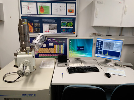
Scanning electron microscopy (SEM)
A scanning electron microscope (SEM) is designed for fast analytical and micro-morphological investigation of surfaces.
The spatial resolution of a SEM covers the range between those of a light microscope and a transmission electron microscope, with our instrument down to 3 nm (30 kV). With a large focal depth, the SEM allows for needle-sharp photographs of smooth and rough surfaces. A back-scattered electron detector displays compositional variation of light and heavy elements across the imaging area. An energy dispersive X-ray spectrometer (EDS) attached to the instrumentation provides quantitative elemental analysis of single spots, line scans and area scans as well as element distribution maps.
Instrumentation
SEM: JEOL JSM-6510 (W filament, 0.5 – 30 kV acceleration voltage)
EDS: Oxford Instruments INCAx-act
Sample Requirements
- maximum sample size: 32 mm in diameter full coverage
- vacuum stable (non-degassing)
- polished and unpolished
- electrically conductive
- for electrically non-conducting samples, two sample coaters are available:
- C-coater: POLARON CC7650 Carbon Coater
- Au/Pd-coater: POLARON SC7620 Mini Sputter Coater

